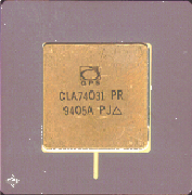
pRAM-256
|
pRAM-256 neurocomputer with on-chip learning |
General DescriptionThe pRAM-256 is a versatile neural network processor with an on-chip learning unit. It offers the flexibility of a software solution with the speed of hardware. Connections between the pRAM neurons are reconfigurable which allows a network's architecture to be modified at any time. The pRAM-256 can complete one pass of the training process, training all 256 pRAMs, in less than 0.25 ms when operating at the maximum clock speed of 33 MHz. Because of the high number of pRAMs supported by the pRAM-256, a typical neural network can be built using a single pRAM Module. Several pRAM Modules can operate in parallel so that larger networks can be built. The pRAM-256 is fabricated using an advanced sub-micron gate array semi-custom technology from GEC Plessey Semiconductors. The use of a 68 pin PGA package allows a compact neural network to be built into existing and future systems. Interfaces to EISA and VME bus systems have been defined and the current PC-based board is capable of carrying up to 5 pRAM-256 chips |
|
Data SheetsData sheets are available in PDF. The data sheets are also available from the links below: pRAM-256 data sheets
pRAM-256 timing and bus signals
pRAM-256 configuration examplesThe information below contains some examples of pRAM-256 implementations.
These examples are not exhaustive, but are to give some hints on building
systems using the pRAM-256. |
|
Applications of the pRAMA PC interface card using the EISA bus has been designed for the pRAM-256
chip. Thus a single pRAM board can be used to investigate many different network topologies.
|