
To make an effective processor, on-chip storage of variables is essential. This storage is provided using registers. The logic gates required to build registers have already been introduced in this course, but have normally been considered to be one-bit storage elements. When we are processing data in bytes, then 8-bit registers will be required.
8-bit registers are formed from a set of 8 flip-flop circuits (e.g. D-type flip-flops sharing a common clock input) where any data which is written to the register stays indefinitely, until it is overwritten by new data.
The way in which data is clocked into a register varies. For example data on the D input can appear at the output:
In the other cases above, the register is an edge-triggered latch where data is strobed by the edge of the clock signal.
A wide variety of latches are available in TTL and CMOS forms for use in computer circuits. These will often be found with tri-state outputs to enable them to be used with a computer bus system.
Other registers are required in addition to data registers. These might be 16-bits wide to hold an address, for example.
Special-purpose registers are required to work with the ALU. In practice, one of the input operands, byte 1, will be stored in a special register called an ACCUMULATOR so that the result of one addition can be carried forward to the next.
We can see how multiple bytes of data can be added together using the structure below. The sequencing circuitry is not shown. The ALU is programmed to perform an ADD operation (in this case) and if successive bytes are presented at the data port, then the accumulative total is held in the ACCUMULATOR register. In a practical system, some means of storing overflows (i.e. the carry bits) will be required.
Here, the result is stored in the accumulator, overwriting any previous data. It derives its name from this accumulating action.
The following sequence will add together two 8-bit numbers.
	1) Load accumulator with operand A
	2) Fetch data operand B
	3) Add A and B in the adder, put the result in the accumulator.
Each step in the sequence will take a few microseconds to execute.
Instead of just adding numbers or performing AND operations, we can require the ALU to do a variety of operations in any sequence. Thus, in addition to the data inputs to the ALU, there are other programming or function select inputs.
Such circuitry is not very complex. An example of such an ALU is found in the 74 series logic family. For example, the 74HC181, is a 4 + 4 bit ALU with 32 programmable functions.
In order to make this ALU into a processor, a means must be provided for presenting the data words at the inputs, storing the output word and applying the appropriate function code at the select inputs for each instruction. Such hardware is incorporated into a microprocessor and the logical sequences for each instruction need not be known by the programmer.
Since we need to read and write data in a computer system, data travels in two directions, to and from the memory chip. In this case, we need bi-directional buffers.
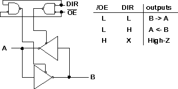
In this example, both buffers can be tri-stated and the direction of data flow is determined by the DIR input. This input will be connected to the R/W line (see later) from the microprocessor.
        A bus is a parallel set of wires (metallisation or conductive silicon internally to
        a chip) which carries information.
The amount of data storage provided internally in the microprocessor is limited. Only a few operands can be stored in the internal registers.
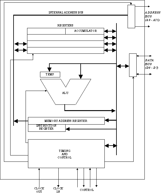
So some means of extending the available storage is provided. External storage elements, or memory, can be read or written to using an extension of the internal data bus. Buffers are provided to interface with external memory chips over an external data bus. These memory chips allow program instructions to be stored, which can be read into the microprocessor at the appropriate time. Results of calculations and data to be input to the ALU can also be stored in this external memory. The arrows on the diagram show that the data bus is bidirectional, that is, data must be able to pass to and from external memory as the microprocessor writes or reads it. Clearly, a control signal is provided to indicate in which direction the data is travelling. This line is called READ/NOT-WRITE or R/W for short. When HIGH, a memory read operation is taking place; when LOW, a memory write (ie. the microprocessor is transferring data to external memory).
Since there will be a large number of external memory locations, we need to specify which one is to be used for transferring data to or from the microprocessor. This is achieved by the address bus. The address bus carries a 16-bit code which uniquely identifies the external memory location we require. Each memory location will only respond to its own code (called its address) and, according to the setting of the R/W line, will take data from the data bus or place data on the data bus. The address bus is unidirectional since it only makes sense for the microprocessor to generate addresses as it is the system controller.
The address bus of 8-bit microprocessors is usually 16-bits wide which allows us to access up to 65536 external bytes of data. As a shorthand, 1024 bytes is called lk bytes; thus 65536 equals 64k bytes.
Accumulators are a special class of register which are closely connected with the ALU such that arithmetic and logical operations can be easily performed on their contents.
Registers are storage elements, some of which have specific functions owing to the way in which they are implemented in hardware or the task they have to perform.
In order that transfers of data occur in an orderly manner, Timing and Control circuits coordinate all such operations. Buffers are controlled by these circuits.
Address and Data Busses exist to transfer data both internally and externally to the microprocessor.