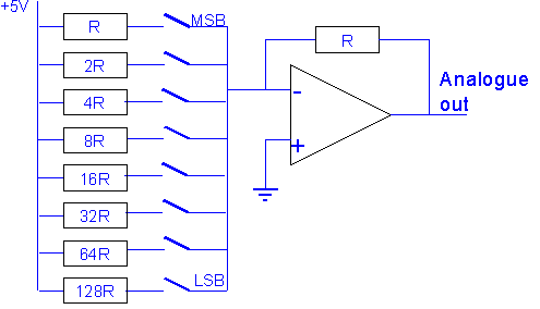

The simplest DAC switches currents in the ratio of 1, 2, 4, 8, 16 etc, i.e. powers of 2. When these currents are summed, the analogue current is proportional to the digital input value. Therefore the analogue output above is proportional to the digital input value.
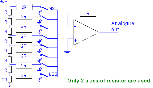
To overcome the difficulty of fabricating resistors accurately over a wide range of values, the ladder structure allows the use of only two resistance values.
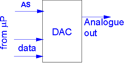
Some DACs may be connected to a microcontroller via a parallel port (PIO chip) where the PIO drives the data lines. Other DACs are microprocessor-compatible so that the data lines connect directly to the data bus and an Address Strobe is used to latch the parallel data into the DAC.

These use a
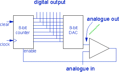
Assume that the counter has just been cleared. The output of the DAC is also zero. The analogue input will be greater or equal to the DAC output and the output of the comparator enables the counter. The counter increments at the clock rate and the DAC output increases as well until the DAC output exceeds the analogue input. At this point, the comparator switches and disables the counter. The digital output can then be read. |
|
If the counter is changed to an up-down counter and the enable input becomes the up-down control, the comparator output is used to drive the counter in such a way that it tracks a changing input signal. In this way, a tracking ADC is formed.
|
These devices convert an analogue signal into a digital one at a constant rate,
dependant on the resolution (number of bits) of the ADC. They employ a single
comparator, which is used sucessively to produce one bit of the digital output.
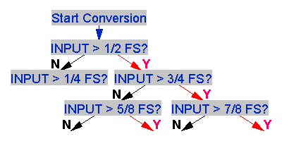
Consider the diagram opposite which shows the input signal level in red. This is first compared with 1/2 full-scale (FS) and a '1' recorded if the input was greater than, or a '0' recorded if the input was less than 1/2 FS. This is the most-significant bit (MSB). To the weight of the MSB, the next most significant bit (1/4 FS) is added for input to the comparator. Again, a '1' or a '0' is recorded. This process repeats until all the bits have been converted. Eight comparisons are required for an 8-bit ADC. |

|
|---|
|
An alternative way of describing the process is shown here. For each red (yes) arrow, a '1' is written to the result and for each black (no) arrow, a '0' is written. |
|
This class of converter is useful when periodic interference is to
be rejected. For example, 50Hz mains interference can be rejected
if the signal is integrated over a multiple of 20 milliseconds.
The integrated signal is then digitised using an incremental ADC (decremental actually). | 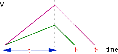
|
|
ADCs can also be obtained which connect directly to the bus.
In this case, the start conversion and conversion done
signals will normally be represented by bits in a control and
status register respectively.
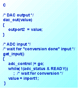
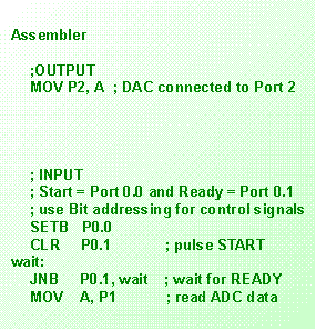
It is important to wait for the conversion to complete after giving the start conversion signal. This is to allow the ADC time to operate, otherwise the data read will be erroneous. Either a software loop is entered, or the ADC's own conversion done signal is checked (this could alternatively be connected to an interrupt input on the processor). | 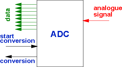
|
|
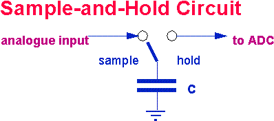
The S/H circuit uses a capacitor to follow the input voltage. When
a sample is required, the switch is moved to the hold position
where it retains an instantaneous value of the analogue signal.
Note that a capacitor takes some time to acquire the input voltage level when the switch is set to sample owing to the exponential charge-up of the capacitor. Therefore, a typical time of 3 microseconds should be allowed for the sample period, followed by the conversion time (e.g. 10 microseconds). In this example, the minimum period between samples is 13 microseconds. |
