An example is given below of an interface using simple latches; normally we will not construct ad-hoc interfaces, but use a purpose-built interface chip such as a peripheral interface adapter (PIA or VIA) for parallel data. One such device, a VIA, is described at the end of these notes and again in the following lecture notes.
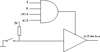
We have two problems logic signals and timing. The logic problem is easily overcome by adding a resistor to +5v. When the switch is open the reistor pulls the output to logic 1 when closed the output is forced to logic 0.
The timing problem requires a little more thought. First we need an output which can be switched on and off - this means a tri-state logic gate or buffer. Then we need to determine when the data should be put on the bus. Presumably we want the switch to be at some memory location not used by other memory. Suppose we are not using the range $8000 to $BFFF (we might have RAM below $8000 and ROM from $C000 upwards). We could therefore choose one of these free locations $8010 for example. This means we want our interface to respond with the switch data when
There are two solutions to this problem which are usually used in conjunction with each other.
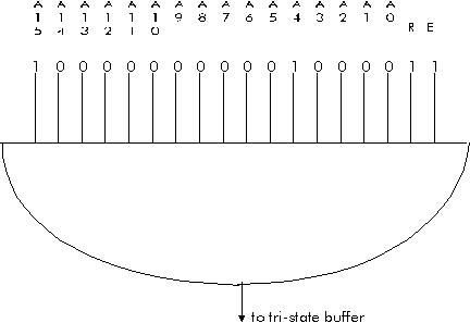
1. Incomplete decoding. The process of selecting the appropriate address is known as address decoding and what we have done here is to completely decode the address. I.e. if any other address appears on the address bus then the interface doesn't respond. But if we look at our system the entire range of addresses from $8000 to $CFFF is unused so we could in theory allow the switch' interface to respond to any or in fact all of these addresses. All we have to do is to make sure that it doesn't respond to addresses outside that range. If we look at how the address space is divided up we see that it is controlled by A15 and A14.
                   A15 A14    Address range        Devices addressed
                    0    0    $0000 - $3FFF               RAM
                    0    1    $4000 - $7FFF               RAM
                    1    0    $8000 - $BFFF            Interface
                    1    1    $C000 - $FFFF               ROM
All we have to do, therefore is to detect when A15 is 1 AND
A14 is zero. The inputs to our AND gate are now only four.
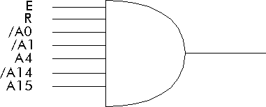
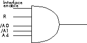
The solution is to add a few more address inputs to our AND gate but not to decode all of them. For example we might add A0,A1 and A4 so that the interface responds to $8010 as originally intended.
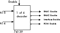
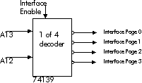
2. Address Paging - The other approach, which as I have already said is often used in conjunction with incomplete decoding is address paging. Here the decoding is done in stages. We might, for example, first create four pages of $4000 locations by decoding A15 and A14
In practice we use a combination and in this particular example we might take Interface Enable with addresses A4, A1 and A0 and of course R into a 5 input AND gate which is a fairly normal size.
The PIA (Peripheral Interface Adapter) from Motorola and the VIA (Versatile Interface Adapter) from Rockwell are typical and popular examples sharing many common features. Each has these two 8-bit parallel interfaces which occupy consecutive locations in memory so that they can if necessary be used in conjunction to provide up to sixteen bits. (Thus a LDD instruction loads the data from both interfaces into D = A:B). Additionally each of the 16 interface connections can be programmed to be either an input or an output connection thus catering for control applications where each line performs a different function (controlling an open or shut valve or detecting the presence or absence of a component on a conveyor belt). This programming is performed as we have already seen using two further registers in the interface. In the case of the VIA these are organised as follows:-
                    Address n       Interface Register B
                            n+1     Interface Register A
                            n+2     Data Direction Register B
                            n+3     Data Direction Register A
Each bit of the Data Direction register controls the direction of
one of the interface connections. Thus DDRA0 controls the
direction of data on line PRA0 and DDRA2 on PRA2 etc.
The address at which the whole interface appears is determined by address decoding as before and also by two Chip Select inputs CS1 and CS2. The first is active high and the second active low which means that "10" on these is required to enable the chip. The advantage of this is that by suitably juggling the address connections to these pins it may be possible in small systems to avoid any additional address decoding. For example connecting A15 to CS1 and A14 to CS2 puts the interface at memory location $8000 (but note that the decoding is incomplete, which means that the interface will also appear at many other addresses.
           A15 A14 A13 A12 A11 A10 A9  A8  A7  A6  A5  A4  A3  A2  A1  A0
            1   0   0   0   0   0   0   0   0   0   0   0   0   0   0   0
           CS1 CS2                                            RS3 RS2 RS1 RS0
The versatility of these devices does not end there. If a
sequence of data is to be transfered to or from an external
device then some sort of handshake mechanism is required to
ensure that data is received correctly. For example if a page of
text is to be sent to a printer then the processor is capable of
sending a new data byte every few instructions by stepping
through memory using the index register. Thus a new byte can be
sent every 10 microsecs. A printer can typically print at 100
characters per sec or one character every 10 millisecs. Thus
there is a difference in speed of 1000 or if the processor is
sending data continuously then 1 character in 1000 will be
printed correctly. To overcome this we use two handshaking
signals which have a variety of names the most common of which
are 'Data Available' and 'Data Accepted'.
          Data Available      This signal is used to indicate that a new
                              data byte is available on the interface lines
                              which requires printing.

          Data Accepted       This indicates to the processor that the
                              printer has printed the current data byte (or
                              at least read the byte into a buffer ready
                              for printing) and is ready for the next one.
The sequence of signals is as follows:-
The handshaking ensures that the processor does not change the data byte before the printer has read it and that the printer does not read data which is incorrect. Although there are many variations on this it can always be carried out using two signals, one from the sending to the receiving device and the other going in the opposite direction.
To enable handshaking to take place the VIA (or PIA) has two Control Signals for each of the two interfaces - these are labelled CAI and CA2 for A interface and CB1 and CB2 for B interface. CA1 and CB1 can only be used as inputs but CA2 and CB2 can be used as outputs (for handshaking) or as inputs (for applications not requiring handshaking).
The operation of the control lines is controlled by a further register in the interface - the Peripheral Control Register, which resides in memory location n + C.
Address n + C Peripheral Control Register
The processor is not normally concerned with the actual logic
level on the input control line. What it needs to know is when a
transition has occurred on the line which then initiates some
action (outputting the next data byte for example). The interface
therefore detects transistions and when such a transition occurs
a flag is set which the processor can detect. In some
applications the transition being looked for is the 1 -> 0
transition and in some the 0 -> 1. Sometimes both may be
important, The control register has a bit which determines which
transition is detected. Another bit does the same thing for CA2
(CB2) when it is used as an input. Obviously there must also be a
bit which determines whether CA2 (CB2) is used as an input or
output and when programmed as an output another bit must
determine what value that output takes up.